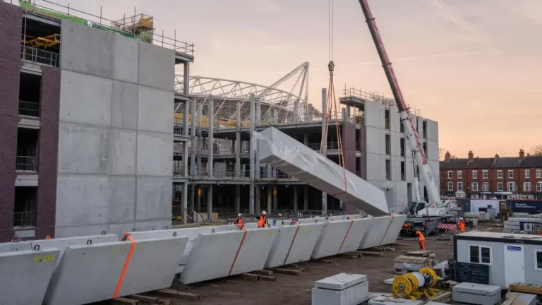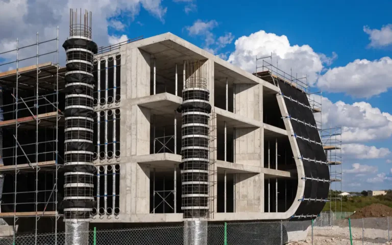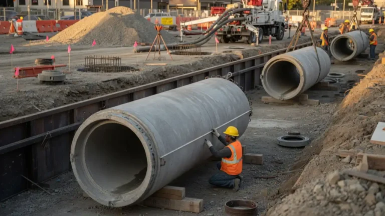

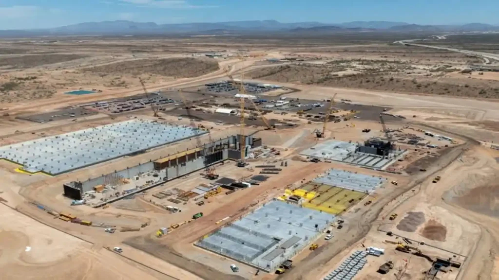
The largest outsourced chip packaging plant ever planned in the U.S. is rising in the Arizona desert, and its construction methods are spreading to other regions.
Tracking Amkor manufacturing sites and packaging technologies by location shows where cleanroom-grade work, precast demand, and skilled-trade budgets are heading next.
Key Takeaways
- Amkor’s $2 billion advanced packaging and test campus in Peoria, Arizona, will be the largest outsourced packaging plant in the U.S. and will create roughly 2,000 jobs.
- The footprint grew from the 500,000+ sq ft first announced to 750,000+ sq ft of cleanroom manufacturing space across two phases.
- Specialized labor is the real bottleneck. TSMC’s first Arizona fab slipped to 2025 because crews with chip equipment installation skills were hard to find.
Kern County Megaprojects Construction 2025 2026
Why should contractors care about a chip packaging plant?
Our analysis suggests this project is less about semiconductors and more about a new class of high-spec building.
According to Construction Dive’s original report on the Peoria facility, Amkor’s first production phase was slated to open within two to three years of the December 2023 announcement.
That phase will handle advanced packaging and semiconductor testing for high-performance computing, automotive, and communications markets.
Apple will be the first and largest customer.
The plant will package and test chips made at a nearby TSMC fab, part of a $40 billion investment covering two Arizona fabs.
When we map Amkor manufacturing sites and packaging technologies by location, Peoria stands out because front-end fabrication and back-end packaging now sit within driving distance of each other on U.S. soil.
What are Amkor manufacturing sites and packaging technologies by location?
Amkor runs a global network, with major packaging, test, and R&D operations across Asia and a growing U.S. presence.
The table below compares the sites most relevant to the Arizona buildout.
| Location | Role / Technology | Key Data | Timeline |
|---|---|---|---|
| Peoria, AZ | Advanced packaging and semiconductor test | $2B; 750,000+ sq ft cleanroom in two phases; ~2,000 jobs | Announced Dec 2023; groundbreaking Oct 2025 |
| Songdo, South Korea (K5) | Advanced packaging plus Global R&D Center | Toured by Arizona Gov. Katie Hobbs | Operating |
| Bac Ninh, Vietnam | High-volume packaging and test | Amkor’s first Vietnam factory | Opened 2023 |
| TSMC Arizona (partner fab) | Front-end wafer fabrication | $40B across two fabs | Fab 1: 2025; Fab 2 (3nm): 2026 target |
Amkor’s official groundbreaking release confirms the campus will complement TSMC’s wafer work for full end-to-end domestic production.
Read this way, Amkor manufacturing sites and packaging technologies by location reveal a clear pattern.
Asia still carries volume, while Arizona carries the strategic growth.
Monarch Black Hawk Hotel Tower Construction: The Ultimate Guide
How does federal funding change the construction picture?
Amkor applied for support under the CHIPS and Science Act, and the Commerce Department set aside $3 billion for packaging investments.
The NIST NAPMP Advanced Packaging Summit materials describe a national network built to move research “from lab to fab.”
Commerce later finalized $1.4 billion in advanced packaging awards, including $1.1 billion to Natcast for prototyping capabilities.
Federal dollars now shape Amkor manufacturing sites and packaging technologies by location as much as customer demand does.
Amkor Manufacturing Sites and Packaging Technologies by Location Spur Builds Tracking Amkor manufacturing sites and packaging technologies by location shows where cleanroom-grade… @SamsungDSGlobal @intel @AmkorTechnology https://t.co/xZiQKO7HIQ
— US News (@Us_news_ways) October 12, 2026
What does this mean for Midwest contractors?
If you’ve been following construction technology trends across the Midwest, this won’t come as a surprise.
Construction industry insiders are noting that chip-adjacent work is spreading beyond Arizona, Texas, and Ohio.
Ancillary suppliers, chemical plants, and logistics hubs follow every fab and packaging campus.
Our team observed that these projects reward contractors who can deliver:
- ISO 14644-1 cleanroom envelopes with tight air-leakage limits
- Vibration-isolated slab-on-grade and waffle slab systems
- Precast double tees and insulated precast wall panels for support buildings and parking structures
- BIM coordination at LOD 400 for dense MEP layouts
- Prefabricated MEP racks and modular utility skids
Watching Amkor manufacturing sites and packaging technologies by location gives Midwest firms a preview of the specs heading toward regional industrial parks.
Town of Dartmouth MA Megaproject Construction 2025 2026
How will this impact your next build?
Expect owners to demand faster schedules, fewer on-site trades, and documented quality control.
Precast and prefab fit that demand because components are cast and inspected in controlled plants.
What’s the step-by-step bid prep for high-tech industrial work?
- Audit your experience. List any controlled-environment, pharmaceutical, or data center projects you’ve completed.
- Upgrade your digital workflow. Move estimating and coordination into a BIM platform that supports clash detection.
- Pre-qualify precast partners. Confirm PCI-certified plants can meet tolerance and lead-time requirements.
- Secure skilled labor early. Sign agreements with electricians, pipefitters, and controls technicians before bidding.
- Track funded projects. Monitor CHIPS award announcements and state economic development boards for upcoming sites.
James Beard President Beard Construction Group Lessons for Precast Concrete Contractors
What should you watch next?
The City of Peoria’s groundbreaking announcement places the campus in the city’s Innovation Core, a district built to draw more suppliers.
We found that every major packaging site attracts a second ring of smaller industrial projects within a few years.
Keep monitoring Amkor manufacturing sites and packaging technologies by location, because the next supplier build could land closer to the Midwest than you expect.